Which pictures were you wondering about? The 3D ones of the boards are a built in feature in KiCAD. When you are in the PCB Editor (pcbnew). You go to View | 3D Viewer.
For the Bus Pirate photos, I used an iPhone w/ SnagIT. The background is a gymnastics mat.
Re-ordered my CE Header board and SensorBoard due to solder mask clearance issue. The most recent version of KiCAD seems to have changd the defaults for the solder mask pad clearance and solder mask pad min width. This changed has caused issues with my 4 most recent boards where the solder mask is “pulled away” from the ground and power planes exposing a ring of copper right near the pads the need to be soldered causing shorts.
Oh yeah! FRAM is great. It’s finally starting to come down in price a little bit, it has been around a long time but the patent is up soon i think. I know TI started putting it into MSP430 chips.
Here you go. In each photo, Left is the new and Right is the old. I haven’t done any soldering yet, but the mask looks the way I would expect now. Huge difference.
You can click on the images to get the full size original.
NOTE: On the Good board, you see a tiny reflection around the through holes. That isn’t an actually spot where the mask is missing. I had to use a flash where I am to help show the missing mask on the bad board.
You can see by the screen shots, the only value I changed was the Solder Mask Clearance. Once I realised what my issue was, I went back on previous boards and saw that this value was also zero. I therefore set mine to zero and checked it carefully against the Gerbers and this worked out fine and has ever since.
I did report the issue 2 different times since it was happening on multiple boards and in both cases it was explained that my settings were the issue. At the time, I didn’t notice the silkscreen. And since changing my settings looks to have resolved the issue, I am hopeful just to move on.
Chris, do you have anyone you connect with to see if the KiCAD issue can be given a new look? It sounds like the current default isn’t a reasonable one and thus will likely cause issues for people new to creating PCBs. I am not sure how I would have handled it if the first PCBs I created from KiCAD cost me money and didn’t work, and I didn’t know how to figure out what was going on or who to talk to about how to fix it.
There are a couple developers over on the KiCad forums, might be a good idea to bring it up there. At the very least, it will give visibility to others as well, should the change take a long time.
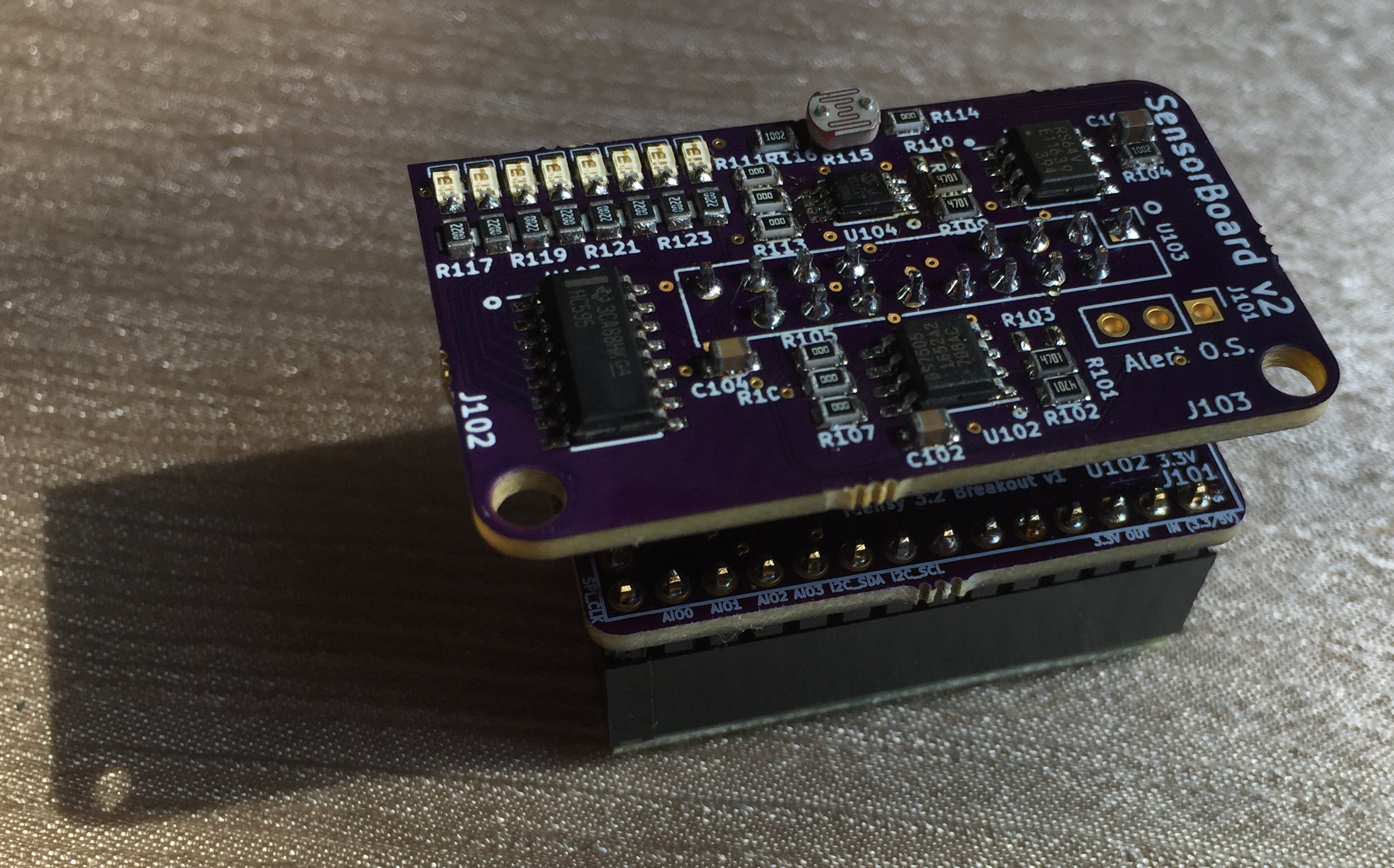
I had time last night to work in the SensorBoard v2. I was able to laser cut the stencil, paste, place, reflow and visually inspect. Next stop will be to plug it in and test. During the fab downtime, I have been writing test applications for all the different sections. This should shorten my bring up time.
Thanks, Chris! Yes, we appreciate any issues being reported to support@oshpark.com, so we can work with the customer to resolve any problems. Our goal is always to produce perfect purple PCBs
I tested each of the Arduino sketches with the SensorBoard v2 and they all worked. They covered both I2C temp sensors, the SPI FRAM, and the analog-read photoresistor ( values from about 20-1020 ).
The only chip I didn’t have a sketch written for yet was the SN74HC595 shift register. I am working on that sketch next.
Thought I would share a design mistake for the TeensyBreakout w/ SensorBoard v2. It turns out it is a good idea to keep in mind the physical design of your boards when you plan to stack them. I thought I had done pretty well, until I needed to press the reset button! That’s right. It took some creative re-purposing of an ink pen by borrowing its refill to sneak in there and press the button. I am thinking the rev 3 SensorBoard needs to either have a hole that goes through every single “shield” or bring a reset button up to at least the Teensybreakout.
I wrote the test sketch for the SN74HC595 and it works. All sections of the SensorBoard v2 have tested as working. My next task will be to write some firmware that takes advantage of all 5 sections. Two temperature sensors, FRAM, photo resistor, and shift register with 8 LEDs.
I relaised this too - I will be exposing the ~RESET on the header in my next project.
Since the CE is general purpose the option would be either use one of its GPIO as the reset or to simply add an addition single Pin Header. The options of exposing it on the CE Header or, as you suggest, give some mechanical access to the Teency reset button do not cost anything extra.