4 or 6 layer PCB stackup for EMI hardening overkill

Looking for some feedback on PCB stackups for EMI immunity for a prototype daughter board to extend 4 traces approx. 4 inches from a 10-pin, 0.1" header on an eval board to some plastic-optical-fiber transceivers, each trace running at 50 MHz for TI’s Fast Serial Interface out of their C2000 MCU line. The fiber transceivers are sitting right next to VFD power electronics so EMI hardening is high on my list of things to look out for.

Rough daughter board specs so far:

  1. Sit atop a TI LaunchPad-XL F280025C evaluation board (LAUNCHXL-F280025C Development kit | TI.com) and connect to the 10-pin FSI (Fast Serial Interface) header.
  2. Route TX-CLK and TX-DATA to two Broadcom AFBR-1629Z DC-50 Mbaud transmitters. Route RX-CLK and RX-DATA to two Broadcom AFBR-2529Z receivers. CLK/DATA pair should have minimal skew, TX and RX channels are independent so all four lines don’t necessarily have to be matched length but will probably try my best anyway.
  3. 2"x3.5" outside dimensions to reach from the FSI header and have the fiber transceivers sit over the LaunchPad’s USB port.

I’ve used this 4-layer stackup for a few boards but mostly for signals <100 kHz
Signal/Ground/PWR/Signal

I came across this article and their idea for 6-layer GND/Signal/PWR/GND/Signal/GND seemed like the overkill I’m looking for.

It looks like the cost of 6-layer on JLCPCB, even with their impedance control option, is still in the budget. Is this overkill or am I on the right track here?

Here’s what I have so far in Eagle:
GND/Signal/PWR/GND/Signal/GND
100mil curved radius miters
yellow traces are layer 2
orange traces are layer 5
trace lengths are all within 0.01mil using the Meander tool (not sure what the LaunchPad eval board does for its traces on the other side of the FSI header but I’m guessing this is as good as I can do?)
Trace with right now is 9mils for OSHPark’s 6-layer thicknesses calculated with Saturn PCB Design’s stripline-asymmetric tool to get to a 49.276 ohm trace, not exactly sure what I need for this.

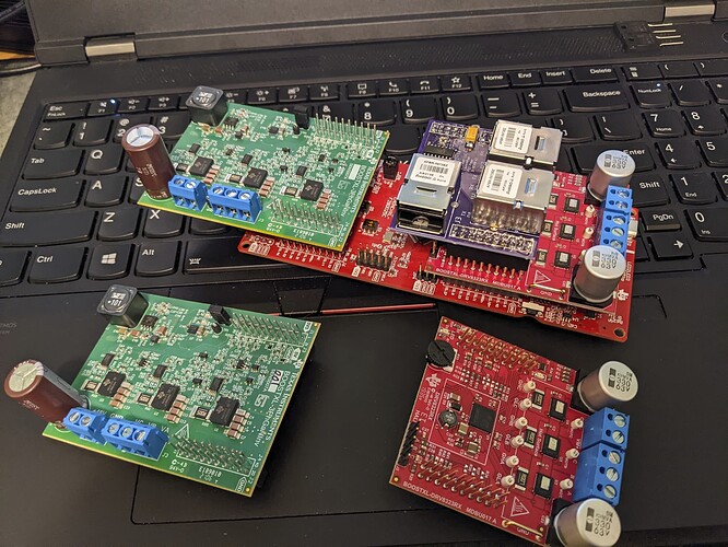
LaunchPad eval board with some more eval daughter boards
LaunchPad is on the bottom
Green daughter card is a TI 3-phase bridge eval board
Red board with the two aluminum polymer caps is another 3-phase bridge eval board
Purple OSHPark board is a first go at an FSI board using Broadcom HFBR-5972 plastic fiber transceivers, pretty cool with LVDS inputs, but FSI turns out to be a burst message, not continuous, so the HFBR-5972’s complained since they’re expecting 8b/10b encoding with no dc bias in the signal or they go into sleep mode.
This new board will be to replace the purple board with the DC-50 Mbaud transceivers which will be friendly to the burst FSI messages.

For some more background,
I’m working up to a test using the TI C2000 series MCU LaunchPad-XL F280025C to try out their Fast Serial Interface (FSI) which is rated for 100Mbit in a daisy-chained network topology. The TX/RX CLK runs at up to 50 MHz and the TX/RX DATA lines are 50 MHz double-data-rate to get 100 Mbit. I’m only going to use one of the two data lines.
.
App note on their daisy-chaining for power converter applications:

The application really needs fiber isolated signaling otherwise TI’s approach using the Cat5 cables with LVDS would be ok. I’m getting more practice with Eagle’s meander tool for trace length matching, this higher

Hi.

I do feel like the 6 layer stackup might indeed be overkill. I’d even argue that if the signal integrity of your design depends on this, then it might be more interesting to work on reducing the emissions of the radiating elements.

First because that’s a step towards a less painful certification process, and second because who’s to say that the other boards you use offer the same level of immunity?

Also, I’d add a fair amount of via stitching between your ground planes.

Regards,

Nicolas

1 Like

Thanks for the input. Comparing to the other boards in the application, I was most concerned with the fairly long 4inch traces to get the mechanical layout needed at the 50 MHz rate. Compared to the clock crystal being right next to the MCU. All other long traces on the board would also be much lower signal rates <=50kHz.
This is also preemptive since the power stage isn’t done yet.

I think you might be unnecessarily worried about these signals, on a handful of points.

  • 50MHz is not “fast” in most of senses relevant for PCB design.
  • 50MHz isn’t actually relevant from an EMI perspective - the figure of merit is bandwidth of the edge, i.e. rise time of that signal. You could have a 1Hz signal that becomes an EMI problem because the rise time is 10ps and therefore has a bandwidth of 35GHz. You could have a 50MHz signal with such a slow rise that there’s almost no harmonic content above 50MHz. In fact, this is pretty typical in high-speed signals, like USB and HDMI and so on - the baud rate of the signal is about equal to the bandwidth of the cable, so the signal itself looks basically like a sine wave instead of a square wave, and has little higher harmonic content.
  • Length-matching on this level is kind of silly. Not necessarily, but the rise time of the LED itself in that transceiver is 5ns, which is about 7.5ft of trace on a PCB worth of propagation delay. Those arent the figures of merit here, but it does give you an idea that even if the maximum allowable skew is 1/10 of that, you’re still talking about 9" worth of allowable mismatch.

But ignoring the fact that this board is definitely going to work no matter how hard you try to mess it up, some EMI pointers (not that I’m an expert here!):

The KEY POINT in designing for EMI performance is to contain the field. That is, the field between your signal and ground. The field will spread outward from every point along your trace until it finds a ground conductor somewhere to carry its own return current. To prevent your PCB from radiating, or picking up interference as well, keep that ground return path as close as possible to your trace at all times. This is why passing high speed traces over splits in the adjacent ground plane is bad: when the return current hits the split, it immediately has to stop, change direction, and go hunting for the nearest path around the split which is who-knows-where. Conversely, to create an antenna, we MAKE a big barrier that the return current has to go around. Ship your signal off a meter or two away from the ground return path and it will spread out for miles into the surrounding space looking for that ground. That’s a radio in a nutshell.

So then, let’s talk about those stackups: you seem to be at least mildly aware that the traditional Sig/pwr/gnd/sig is “bad” from an EMI standpoint. The REASON, going back to the point above, is that on that first layer, adjacent to the power plane, any signal has a long journey to undertake hunting for a return path on the ground layer two away. The “easy” solution, since 4L boards are basically as cheap as anything these days, is to change the power layer to ground: sig/gnd/gnd/sig, then route your power on the signal layers. If you don’t have a ton of different rails, it typically isn’t much more difficult, and then every signal and power path becomes a neat, well-constrained transmission line between start and finish with little reason to radiate.

An alternative that can be even better is gnd/sig/sig/gnd, where you use ground pours on the outer layers as a farady cage. Of course the problem here is that your board has pins, so there are going to be a bunch of holes all over that structure. Also it’s just harder to route everything with all the space vias AND pads take up.

Anyway, long story short, you could PROBABLY build the board you’re describing on 2 layers and pass EMI with appropriate precautions taken (ground pour on both layers with plenty of stitching vias, especially near where traces cross each other).

You can DEFINITELY build that board with 4 layers, and since it’s all through-hole, GND/SIG/SIG/GND will definitely work great. Again, you want stitching vias sprinkled all around, basically to provide bridges for stray fields you didn’t anticipate.

2 Likes

No EMC expert here, but I believe this is ok. If you place ceramic capacitors between pwr and gnd spread out, the pwr plane is a good as the gnd plane as image/return path. Right?

1 Like

:+1: thanks

With the ridiculously low number of signal traces, what about a PWR/GND/SIG/GND 4-layer with via stitching the two grounds together. That leaves room on the top for surface mount VCC decoupling parts next to the transceivers without cutting up the ground layers. All with plenty of room on the single signal layer for the 4 main signal traces

Right, but only to the extent the capacitors are a low-impedance path (and they often aren’t! Lots of parasitic inductance!) If you’re trying to provide a return current path at GHz, two via barrels and a ceramic cap’s parasitic inductance may well not cut it. Whether that’s more of an issue for EMI or SI is for you to figure out in the lab/chamber.

For instance, you can get around the problem entirely, and just treat any old contiguous power plan as a return current path, as long as the ground plane is so close to the power plane that the whole thing is one continuous parasitic capacitor. 3M C-Ply exists exactly for this sort of thing - it can be manufactured as thin as 8um, and has some ridiculously high dielectric constant such that 1) you get great distributed power supply rail capacitance for the sake of decoupling near power pins and 2) you can mostly treat the contiguous power plane as a return current path.

Otherwise, you’re stuck with caps and all their parasitics. Or of course you can do nothing and just hope.

It could certainly work, but if you’re going to put all the signals on the same layer, you’ll have to via out to one of the other layers where they cross, and you’ll have to make sure there are vias nearby those transitions for gnd current as well. You have to ask yourself whether it’s better to have all the signals sandwiched inside grounds but poking through them to cross over, or whether it’s better to have continuous unbroken impedance paths on separate layers.

For this design, you necessarily have holes in outer layers where the pins poke through, and where you mount any decoupling caps (I’m assuming there are no other chips on this board that you haven’t mentioned?)

The decoupling caps don’t really matter in that sense, unless for some reason you run the data tracks directly under them (and why would you? Don’t.) In my view, GND/SIG/SIG/GND and SIG/GND/GND/SIG are equally easy to route, and you’re just adding headaches by trying to use a separate power plane.

I normally do that and select the Stackup for minimum distance between GND and pwr

That is a very good HF capacitor. And the plane is low inductance also, so some 1nF caps spread out are good for 500MHz

We’re in untested speculation realm for me here, but my impression is, if you’re talking about a 4-layer stackup and traditional dielectrics, that’s probably prioritizing the wrong things. You end up with close L2/L3, but not actually close enough to provide any real distributed capacitance or coupling, in trade for widely-spaced L1<>gnd and L4<>pwr. In other words, I think that stackup gets you worse L1 SI/EMI, much, much worse L4 SI/EMI, and no real decrease in PDN impedance to show for it.

I think, but don’t know, that this is why most 4L stackups are a fat core with prepreg+foil laminated onto the outer layers, when you’d think 2 cores and one prepreg in the middle would be easier to fab.

1 Like

Rick Hartley has some detailed thoughts on this subject – some links and notes:

1 Like

Pardon me if this is a dumb question – but do you have to have the RX pairs and TX pairs in the order you have it drawn? If you can swap RX1/RX2 and TX1/TX2 (or mount the part on the secondary side), wouldn’t you be able to get rid of the line crossings?

This FSI interface sounds interesting. Going to give it a look. Thanks for sharing details about your project!

1 Like

Excellent video, seen it before. Feranec has a lot of good stuff

About the video, would be nice if there were figures to support the claims

It is a good question. The only orientation I wanted was that the inner signals be the same such that a straight-through-duplex (not crossover) plastic fiber cable assembly can be used to chain the boards together. After sleeping on it thinking about two signal layers to deal with the crossover, I also came to the conclusion of flipping the RX1/RX2 and TX2/TX1 to get rid of the crossover.

Hartley is excellent, but you have to keep in mind that his perspective is one of extremely high-speed bleeding-edge design, where inter-plane distributed capacitance and via inductance are major factors. It’s good to have an understanding of these parasitics, but if you’re working at frequencies an order or two of magnitude lower they may be a lot less significant. Of course, the principles of transmission lines and return current flow that he discusses apply anywhere above audio.

2 Likes

Actually, I think you probably have enough clearances to your trace to maintain the current ordering. You just have to route the traces to reach around to make the connection without crossing.

I have listened to the gods speak on Altium-sponsored talks. I love their stuff, but also started to realize that their clients/target audience operate at a level way more sophisticated (and $$$) than what I typically do (and what my clients will pay for). This extends to the detailed SPICE modeling that was being encouraged so that entire systems can be simulated… Yeah, no, that doesn’t work for most projects that I touch!

2 Likes