While learning and getting a hang of KiCAD for the first time, I came across a rather unusual scenario. In PCBnew traces are not snapping to the pads of any component (whether it is a TH or smd component). I know it will have a very easy fix (that’s what i presume) but for a newbie, I need your help.
Hi Piyush,
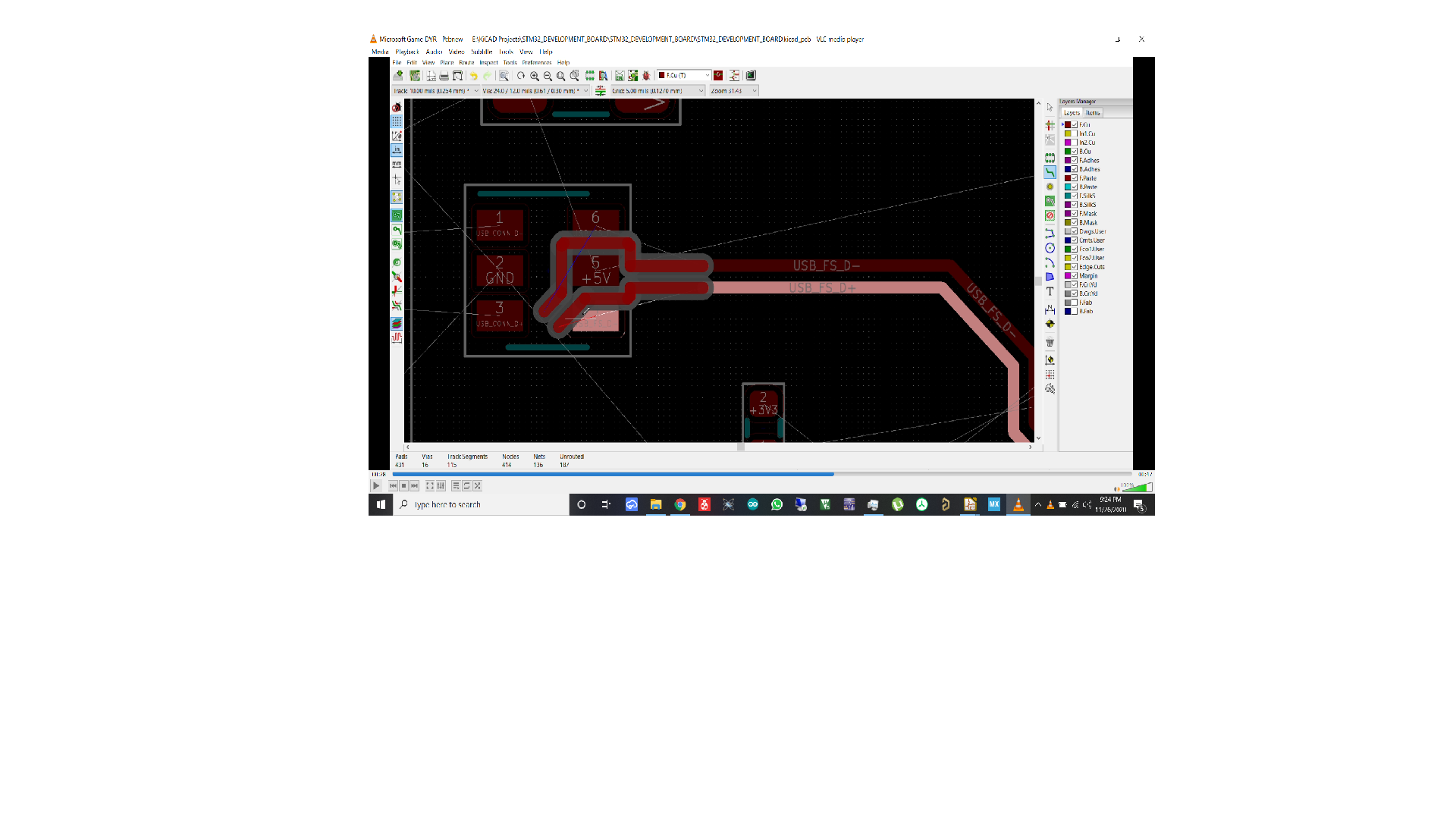
Could you post a picture of the problem? Is it the same over the entire board, or is it just near a corner? There is a known but with regards to corners.
This is an annoyance with KiCad. It won’t snap to a pad unless the pad is centered on a grid node. There are a few workarounds:
Set your grid really fine and snapping will work more often.
Double-click when the trace is inside the pad. This seems to terminate the trace and then add a small segment that does snap to the pad center.
Click when the trace is inside the pad and then hit Esc to terminate.
Hit the “End” key under Windows (not sure if there’s a Mac hot key) to end the trace right where you have it at the moment, presumably inside the pad.
Unlike some other CAD tools, KiCad does not logically “attach” traces to pads - there is no “rubber-banding” where you can drag a component and its attached traces come along with it. Traces just lay where you put them, and if there’s enough copper overlap the rules checker deems them connected.
I’ve read that improvements in this area are coming with v6.
Heh. I’ve used Kicad for many years and never knew this since I’ll always snap components in place on a grid. I actually had this on a board recently and on Mac, you just draw the trace and then tap ESC to finish off.
You know what, I was doing the same thing (get into a pad and hit esc or right-click). I was so frustrated doing this because it was not allowing me to route a proper differential pair.
The fact about the grid size I use 5 mils for the component placement and 1 mil for routing. And I use external libraries for the footprint (downloaded them from ComponentSearchEngine).